Phase III – Focal Topics
Phase III – Focal Topics
For the third funding period, we again defined three research themes as focal topics, which are slightly modified and go a step further than those proposed for the second funding period. The implementation of focal topics is based on the fact that particular themes (a) constitute hot subjects and represent important challenges for carbon allotrope research, (b) require complementary expertise by several of SFB 953 PIs across different disciplines, and (c) have already proved to be very successful throughout the preceding funding periods – especially in terms of prolific collaborations documented by e.g., a multitude of high-quality joint publications. The focal topics are as follows:
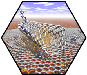
 The different – and at the same time tunable – properties of 0D fullerenes, 1D nanotubes, 3D graphene, and other carbon-rich building blocks combined with the increasing knowledge about precise processing techniques offer the unprecedented challenge to construct nanostructured inter-carbon hybrids. The possibilities of both structural variations and properties engineering are, in principle, limitless. Next to the development and perfection of supramolecular and physicochemical construction principles, which are fundamental and very exciting on their own, new perspectives for practical applications also arise. All-carbon electronics, for example, would offer benefits such as high stability, low-price processing, recyclability, and tenability. In the first and second funding periods, we have already demonstrated that prototype architectures containing e.g., fullerene derivatives, carbon nanotubes, and graphene building blocks can be constructed. It is now our intention for the third funding period to further explore this enormous potential and push the construction and characterization of Inter-SCA-Architectures a considerable step forward.
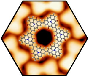
 On-surface covalent chemistry represents a potent alternative for the bottom-up construction of various carbon-based architectures, which are otherwise inaccessible through conventional synthetic methods. This process can also be monitored by scanning probe microscopy techniques. Moreover, the approach appears to be particularly attractive in the context of carbon-based molecular electronics, since the respective nanostructures can be fabricated directly on a surface. This field is currently experiencing a dynamic expansion, as our team and others alike recently demonstrated the rational construction of nanographenes, nanoribbons, fullerenes, and nanotubes. In the first and second funding periods we have accomplished various families of successful concepts for on-surface SCA chemistry. We have, for example, considerably broadened the access to new precursor molecules for on-surface transformation to SCAs and other carbon-rich nanostructures. For example, we have already achieved highly-ordered, two-dimensional, covalent networks pores, and provided the initial evidence for the on-surface synthesis of graphyrins. We have also provided fundamental contributions towards topological covalent chemistry of single-layer graphene deposited on various surfaces. Based on these pioneering results on-surface supported carbon architectures (isocylic and heterocyclic), we will carry the highly attractive opportunities for surface-mediated SCA chemistry (0D, 1D, and 2D) a considerable step forward. We are now in the position to manufacture various families of hemispherical buckybowls (nanotube seeds), graphenoid nanoribbons, carbon nanotubes of defined chirality, porous 2D-heterographenes, and other atomically defined carbon nano-architectures. At the same time, we will accomplish the spatially resolved covalent surface patterning of graphene which will open a new chapter in the field of SCA research.
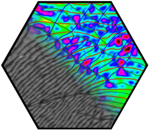
 In the first two funding periods, we have realized that defects, for example, in graphene play a fundamental role with respect to the precise physical and chemical behavior. Whereas initially we concentrated on structural and physical phenomena, such as bilayer graphene stackings, we will now extend our joint exploration and evaluation of defect effects also to chemical reactivity and topochemistry. For example, we have realized that defects in single-layer graphene (edges of hole defects in the plane) strongly activate the adjacent C atoms of the graphene lattice for covalent-addend binding. Such a chemical activation will be used for the defined pattern functionalization (2D-structuring) of graphene. Our joint efforts will also focus on chemical synthesis and the study of defined molecular systems representing the fragments of defect graphene and other SCAs in order to understand the impact of such structural imperfections on the electronic properties and reactivity. We will also continue the successful research on dislocations and related extended defects in bi- and few-layer graphene. Based on the unique in situ mechanical cleaning procedure for graphene and the direct manipulation of dislocations inside the electron microscope, both established in the second funding period, we are now able to study the structural and functional properties of individual defects in predefined configurations. This includes electrical measurements on single dislocations (domain walls), as well as ultrafine force measurements of lattice friction associated with the in-plane movement (glide) of dislocations. By this methodology, we expect to gain insight into the energy landscape of interlayer interaction (Peierls potential) and its effect on the structural and functional properties of these unique defects. We will furthermore focus on the properties of sessile “threading dislocations” penetrating through one of the two graphene layers, and on dislocation nodes containing well-defined areas of AA stacking. Further studies will address highly defective graphene layers grown in situ on top of precleaned graphene layers. By combining the unique structural control and microscopic characterization of defects with complementary Raman spectroscopy studies, we expect to gain new insight into the fine details of defect bands in Raman spectra. This also holds true for twisted bi- and few-layer graphene, for which large-area mapping of domains with precise twist-angle determination is now possible inside the scanning electron microscope, using our novel low-energy nanodiffraction (LEND) setup established in the second funding period.

